The 3 phase VFD circuit diagram that I’ve introduced can be effectively employed to control the speed of a variety of 3 phase AC motors, whether they are brushed or brushless.
3 Phase VFD Circuit
To construct the suggested 3 phase VFD circuit, you’ll need to implement the following critical circuit stages:
- PWM Voltage Controller Circuit: This is the heart of the circuit, responsible for generating the variable frequency output. It’s achieved through pulse width modulation (PWM) techniques, allowing precise control of the motor speed.
- 3-Phase High Side/Low Side H-Bridge Driver Circuit: This stage involves driving the 3 phase motor through high side and low side switches in an H-bridge configuration. This allows the motor to be powered in both directions and at varying frequencies.
- 3-Phase Generator Circuit: This component generates the 3 phase AC supply, which will be later fed into the H-bridge. The frequency of this AC supply is controlled by the PWM circuit, and thus, the motor’s speed.
- Voltage to Frequency Converter Circuit: This is crucial for establishing the V/f (Voltage to Frequency) ratio, which ensures that the motor operates optimally. It plays a significant role in the speed control mechanism.
Now, explain into the functionality of each of these stages:
- PWM Voltage Controller Circuit: This section generates varying PWM signals, which ultimately determine the frequency and voltage applied to the motor. By controlling the width of these pulses, the effective voltage and frequency seen by the motor are adjusted, hence controlling its speed.
- 3-Phase High Side/Low Side H-Bridge Driver Circuit: This stage is responsible for delivering the varying AC supply generated by the generator circuit to the motor’s terminals. It ensures that the motor’s direction and speed are controllable by the generated signals.
- 3-Phase Generator Circuit: The generator circuit produces the fundamental 3 phase AC waveform that feeds into the H-bridge driver. By modifying the frequency of this AC signal through PWM control, the motor’s speed is modified accordingly.
- Voltage to Frequency Converter Circuit: This component is pivotal in maintaining a consistent V/f ratio. It helps in maintaining the motor’s performance characteristics across different speeds.
By intricately integrating these stages, the proposed 3-phase VFD circuit empowers you to dynamically control the speed of 3 phase AC motors. The PWM-based frequency and voltage adjustments, combined with the H-bridge setup, generate the desired motor performance. This type of circuit is widely utilized in various applications across industries due to its versatility and efficiency in motor speed control.
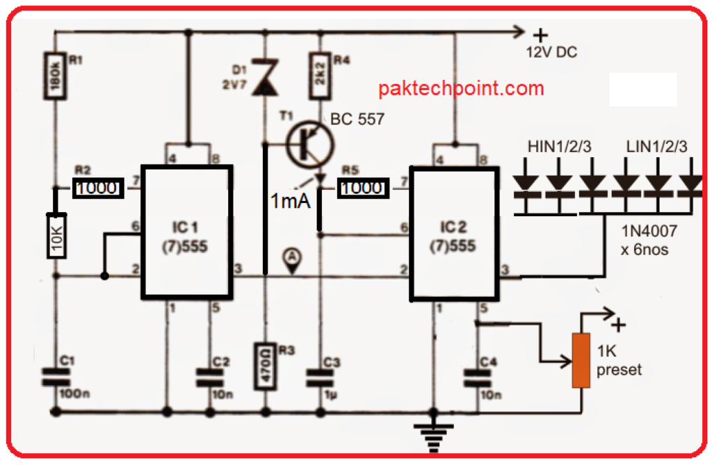
The following circuit diagram showcases a 3 phase adjustable frequency drive, focusing on the PWM generator phase. This phase is responsible for producing varying PWM outputs at pin 3 of IC2 based on the potential applied at pin 5 of the same IC.
The 1K preset featured in the diagram serves as the RMS control knob. It enables precise adjustments to achieve the desired proportional output voltage through the PWMs at pin 3 of IC2.
This configuration is designed to generate an output that corresponds to the mains’ 220V or 120V AC RMS.
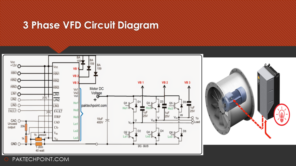
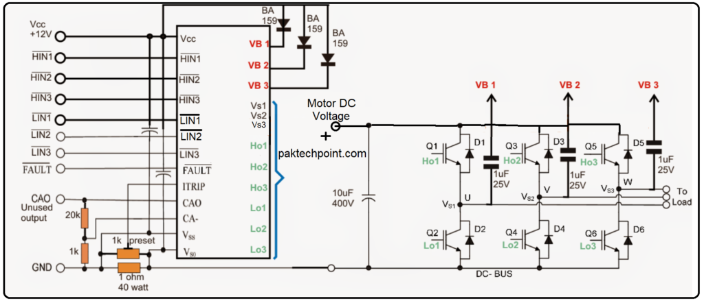
The subsequent diagram illustrates a single-chip H-bridge 3 phase driver circuit employing the IC IRS2330. The design seems relatively straightforward because many complexities are handled by the IC’s built-in advanced circuitry.
3 Phase VFD Circuit Functions
Here’s how the system functions:
- A well-calculated 3-phase signal is applied to the HIN1/2/3 and LIN1/2/3 inputs of the IC via a 3-phase signal generator stage.
- These inputs of the IC can also be integrated with the PWM output from the earlier phase. This helps regulate the required voltage across the IGBTs or MOSFETs connected to the 3 phase motor.
- This regulation ensures that the motor attains the desired speed as per the settings, which can be adjusted using the 1K preset in the initial diagram.
In essence, the combination of these stages constructs a 3 phase adjustable frequency drive. The PWM generator phase facilitates voltage control, while the H-bridge driver stage, supported by the IC IRS2330, efficiently manages the motor’s speed and direction. This comprehensive approach offers a streamlined solution for controlling 3 phase motors in various applications.
Below diagram shows 3 phase signal generator circuit.
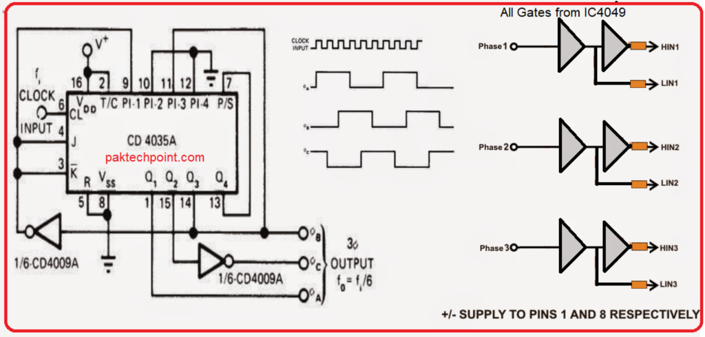
The 3-phase generator section utilizes specific CMOS chips, CD4035, and CD4009, meticulously arranged to generate accurately proportioned 3 phase signals across the indicated pin configurations.
The frequency of these 3 phase signals is determined by the provided input clocks, which need to be six times the intended 3 phase signal frequency.
To illustrate, if the target 3 phase frequency is 50 Hz, then the input clock frequency should be set at 50 x 6 = 300 Hz.
This arrangement implies that by altering the input clocks, the operational frequency of the driver IC can be modified, subsequently leading to a change in the motor’s operational frequency.
However, considering that this frequency adjustment needs to be automated in response to varying voltages, the inclusion of a voltage to frequency converter becomes imperative.
The following stage delves into the construction of a basic yet precise voltage to frequency converter circuit, crucial for the seamless implementation of the entire setup.

The voltage to frequency converter circuit employs an IC 4060, and its frequency-dependent resistance is influenced by an LED/LDR assembly for the desired conversions.
The LED/LDR assembly is enclosed in a light-proof enclosure, with the LDR positioned across a 1M frequency-dependent resistor of the IC.
Due to the linear nature of the LED/LDR response, varying illumination of the LED on the LDR leads to a corresponding change (increase or decrease) in frequency at pin 3 of the IC.
The full scale deflection (FSD) or the voltage-to-frequency (V/Hz) range of this stage can be set by properly configuring the 1M resistor or the value of capacitor C1.
The LED is illuminated through the PWMs generated by the first PWM circuit stage.
As the PWMs fluctuate, the LED brightness also changes, resulting in a proportional increase or decrease in frequency at pin 3 of the IC 4060 in the above diagram.
This varying frequency from IC 4060 now needs to be integrated with the clock input of the 3-phase generator IC CD4035.
These stages collectively form the core components for constructing a 3 phase VFD circuit.
Now, it’s important to discuss the concept of the DC BUS required to supply power to the IGBT motor controllers and the setup procedures for the entire design.
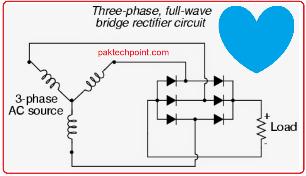
The DC BUS utilized across the IGBT H-bridge rails can be generated by rectifying the provided 3-phase mains input using the configuration shown below.
The IGBT DC BUS rails are connected at the points labeled “load”.
3 phase DC rectifier circuit. For a single-phase source, rectification can be achieved using a standard 4-diode bridge network configuration.
How to Implement the Proposed 3 Phase VFD Circuit
Follow these steps for implementation:
- Apply the DC bus voltage across the IGBTs (without connecting the motor) and adjust the PWM 1k preset until the voltage across the rails matches the required motor voltage characteristics.
- Then, adjust the IC 4060 1M preset to fine-tune any of the IC IRS2330 inputs to achieve the necessary frequency level based on the motor’s requirements.
- Once the above steps are completed, connect the specified motor and provide it with various voltage levels, V/Hz parameters, and set it for automatic V/Hz operations as per the motor’s requirements.